Næxon Learning Center · Fundamentals · Beginner
Terafab is a planned semiconductor manufacturing project associated with Tesla, SpaceX and xAI. Its purpose is to produce advanced computer chips for artificial intelligence, vehicles, robots and potential space-based computing systems. The project’s central idea is to combine logic-chip manufacturing, memory production and advanced packaging within one integrated operation.
For someone coming from refineries, power plants or industrial construction, the useful starting point is the word fab. It means a semiconductor fabrication facility: a factory that manufactures microscopic electronic circuits on silicon wafers. Behind those tiny circuits sits an enormous industrial operation involving electrical distribution, piping, water treatment, ventilation, process equipment and precision controls.
What would Terafab produce?
The project describes three major parts of its manufacturing plan: logic, memory and advanced packaging. Logic chips perform calculations and execute instructions. Memory stores the information those processors need. Advanced packaging connects semiconductor components into a working assembly, allowing processors and memory to communicate efficiently.
That combination matters because an advanced AI system needs more than a powerful processor. Its performance also depends on how quickly information moves between components. Terafab’s proposal brings these manufacturing activities together to support a more integrated chip supply. Its announced applications include Tesla’s vehicles and Optimus robots, along with chips intended for space computing. These remain project goals rather than evidence of completed production capacity.
How does a chip factory actually make chips?
Manufacturing begins with a silicon wafer, a thin, round substrate on which many chips can be produced together. Specialized equipment repeatedly adds materials, creates patterns and removes selected areas to build electronic structures.
Lithography transfers extremely small patterns into a light-sensitive coating. Deposition adds thin layers of material. Etching removes material where the process requires it. Other steps alter electrical properties and create connections. Manufacturers repeat and carefully align these operations to build the finished circuitry.
Think of a complicated construction drawing reduced to microscopic dimensions and built in many precisely aligned layers. A tiny misplaced feature can affect whether a circuit works. That is why semiconductor manufacturing depends on measurement and process control throughout production.
Why does the building require so much infrastructure?
The manufacturing tools need continuous supplies of electricity, ultrapure water, gases and chemicals. Intel’s description of a conventional fab shows these services reaching the cleanroom through a complex network of piping and wiring from the supporting levels below.
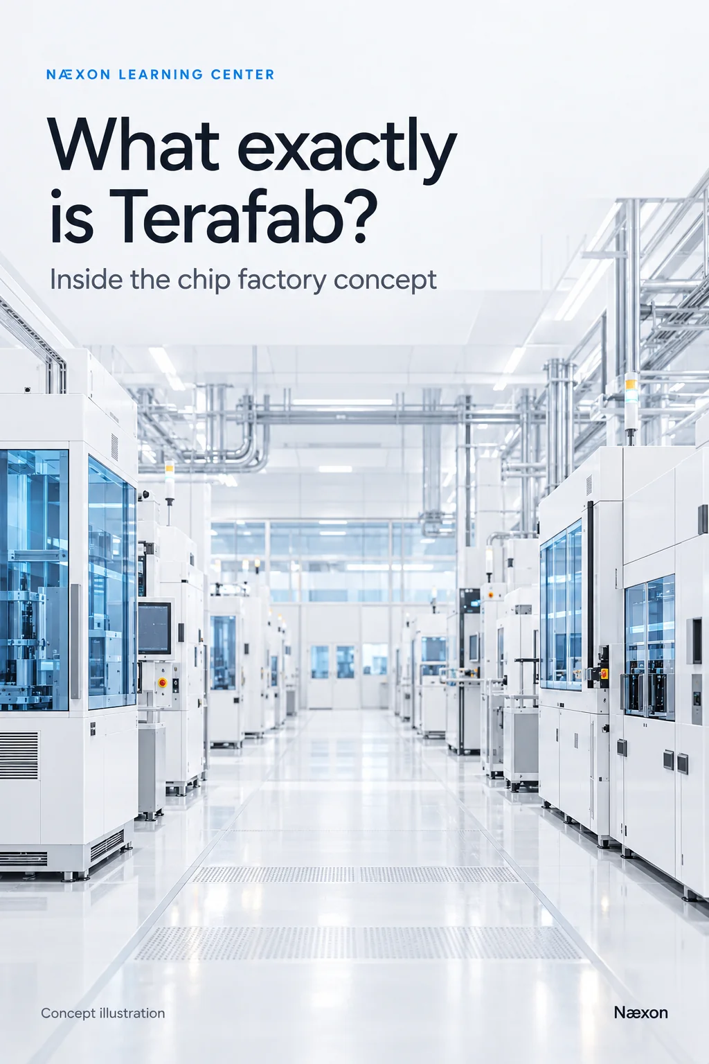
The cleanroom is only the most visible part of the operation. Utility areas and equipment spaces support the production floor, while air-handling systems control the environment around the wafers. A large chip factory therefore requires much more than a clean building filled with machines. It needs coordinated industrial systems that operate reliably together. These are general fab requirements, not a published Terafab equipment specification.
What makes a cleanroom different?
A cleanroom controls airborne contamination around sensitive manufacturing processes. Filtered air moves through the production space in a controlled pattern. Intel describes air entering through ceiling filters, moving through the cleanroom and passing through perforated floor tiles into the level below.
The goal is to protect the manufacturing environment from contaminants that could interfere with production. For a tradesperson, this means cleanliness becomes part of installation quality. Work methods must suit the particular cleanroom and process requirements; practices acceptable in an ordinary mechanical room may be unsuitable around sensitive production equipment.
Why is ultrapure water important?
Ordinary treated water is not automatically clean enough for semiconductor processing. Fabs further purify incoming water to meet the requirements of manufacturing equipment. Intel describes municipal water being treated to ultrapure levels before it reaches tools on the cleanroom floor.
For a pipefitter, the lesson is that a pipe’s purpose includes preserving the quality of what flows through it. Correct installation is about more than pressure containment and avoiding leaks. Materials, cleanliness and handling requirements depend on the service and the approved project specifications.
Is Terafab the same thing as a data center?
A semiconductor fab manufactures chips. A data center operates computers containing chips. The facilities occupy different positions in the computing supply chain, even though both need substantial electrical and cooling infrastructure.
Terafab’s stated role is manufacturing the chips that could support AI applications on Earth and in space. Its space-computing ambitions should not be confused with a claim that the chip factory itself would operate in orbit.
Where is the project planned?
An August 6, 2026, announcement from the Texas governor’s office identified Grimes County as the location for a SpaceX semiconductor fabrication facility associated with Terafab. The state described the first phase as representing more than $16.8 billion in capital investment and an expected 3,000 new jobs.
Those figures describe an announced development commitment and projected employment. They do not establish that every phase is complete, every construction package has been awarded or every projected position is currently open. The announcement specifically identified engineering, technician and plant-operator roles among the expected employment categories.
What does this mean for industrial trades?
Based on the systems used in conventional semiconductor fabs, a project of this type can involve mechanical installation, electrical work, instrumentation, equipment setting, utility construction and commissioning. That is an inference from fab infrastructure—not confirmation of Terafab contractor assignments or hiring openings.
Refinery and power-plant experience provides a useful foundation for understanding how an industrial facility depends on interconnected systems. Moving into semiconductor work also means learning the project’s specific cleanliness, documentation and installation requirements. A familiar-looking pipe, valve or equipment connection may serve a very different process.
Field Rule: Understand the service before the installation
When studying a fab drawing, ask what the system supplies, which equipment depends on it and what conditions must remain controlled. A cooling-water line, chemical supply and high-purity process line should not be treated as interchangeable just because all three appear as piping on a drawing.
Knowledge Check
Explain the difference between manufacturing a chip and operating it inside a computer. Then identify the three manufacturing areas in Terafab’s proposal: logic, memory and advanced packaging.
Practical Exercise
Choose one familiar industrial system—electrical distribution, cooling water or ventilation. Sketch its path from the utility source to the equipment it serves. Mark where a loss of power, flow or environmental control could interrupt production. That exercise connects familiar field experience with the infrastructure behind semiconductor manufacturing.